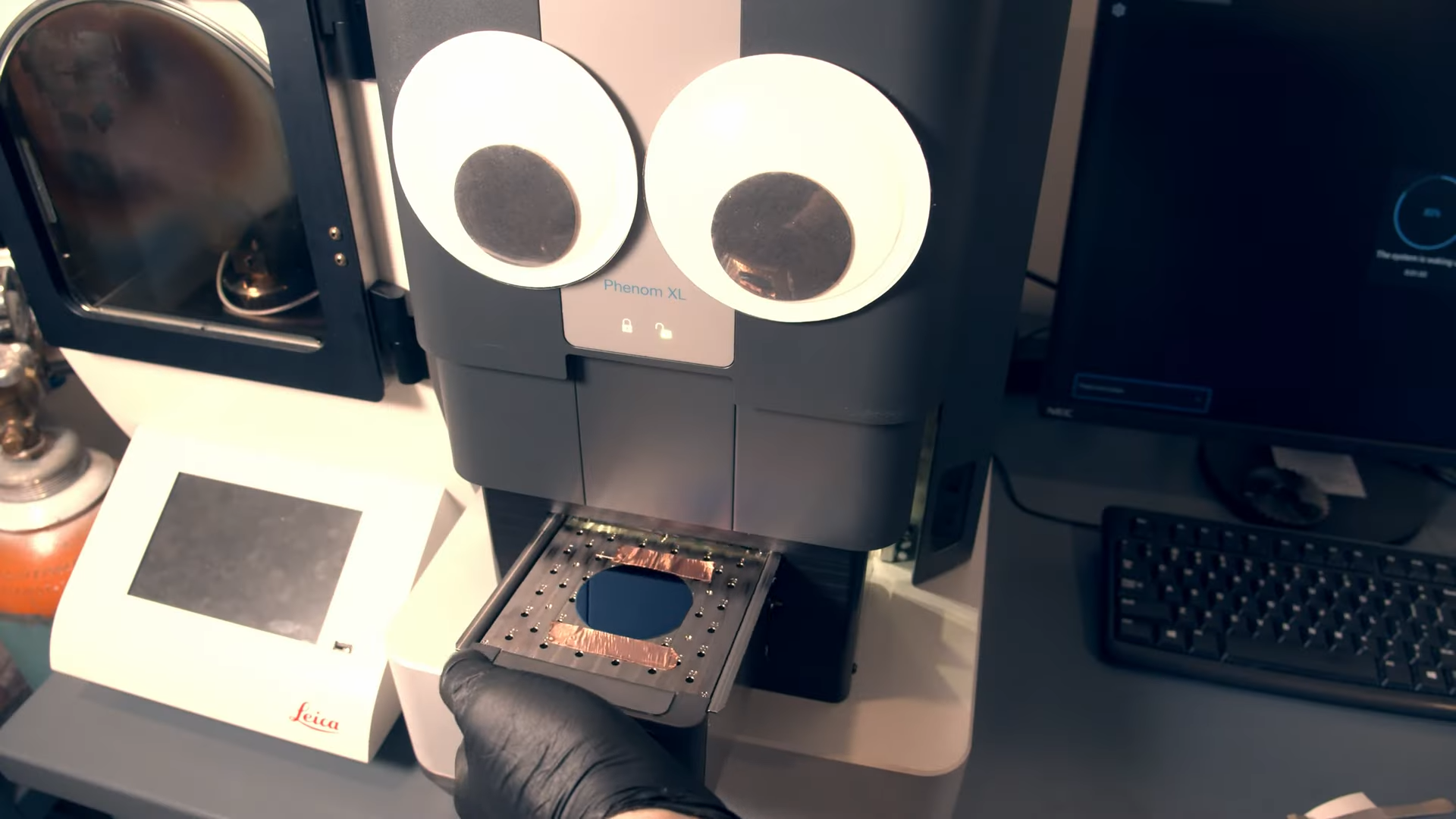
If you have ever tried writing your name on a grain of rice and thought, “Well, that was unnecessarily difficult,” welcome to the universe of electron beam lithography. Except here, the “rice” is silicon, the “pen” is a beam of electrons, and the shapes can be so tiny that a human hair looks like a redwood tree wearing a sweater. Using electron beams to draw tiny shapes onto silicon is one of the most precise methods in modern nanofabrication, especially when researchers need features far smaller than what ordinary optical techniques can comfortably handle.
The main keyword here is electron beam lithography, often shortened to e-beam lithography or EBL. It is a direct-write technique used to create nanoscale patterns on silicon wafers and other substrates. Unlike photolithography, which uses light and masks to transfer patterns, EBL steers a focused stream of electrons across a resist-coated surface. In plain English: it draws with charged particles instead of ink. Very expensive, very fussy, very cool ink.
This technology is not the tool used to mass-produce every chip in your phone. For high-volume semiconductor manufacturing, optical lithography and extreme ultraviolet lithography usually dominate because they can expose large areas quickly. Electron beam lithography is slower, but it shines when precision, flexibility, and experimental design matter more than speed. It is the favorite pencil of researchers building prototypes, quantum devices, silicon photonics, nanosensors, metasurfaces, nanoelectromechanical systems, and other structures that sound like they belong in a superhero’s lab.
What Is Electron Beam Lithography?
Electron beam lithography is a nanofabrication process that uses a tightly focused beam of electrons to write patterns onto a material coated with an electron-sensitive resist. The resist acts like a temporary stencil. After exposure, the pattern is developed chemically, leaving selected areas open or protected. Those openings can then guide etching, metal deposition, lift-off, or other processing steps.
Silicon is a popular substrate because it is the backbone of modern electronics, integrated photonics, MEMS devices, and many research platforms. A silicon wafer is flat, clean, stable, and compatible with a long list of fabrication steps. When engineers want to create tiny silicon waveguides, nanowires, resonators, quantum dot gates, or alignment marks, EBL gives them a way to place features exactly where they need to go.
The Basic Idea: A Nanoscale Pen Plotter
Imagine an old-school pen plotter drawing a design on paper, except the paper is a wafer, the pen tip is an electron beam, and the drawing is measured in nanometers. The system takes a digital layout file and converts it into beam movements. The beam scans across the resist and exposes only the desired regions. Because electrons have much shorter wavelengths than visible light, EBL can define extremely small features.
Of course, “just draw it with electrons” sounds easier than it is. Electrons scatter. Resists behave differently depending on thickness, dose, temperature, and chemistry. Silicon can charge if the surface is insulating. The beam must be calibrated carefully. Alignment must be painfully precise. In other words, EBL is like calligraphy performed during a tiny earthquake while the paper occasionally argues back.
How Electron Beams Draw on Silicon
The EBL process usually begins with a clean silicon wafer or silicon-based sample. The surface may be bare silicon, silicon dioxide, silicon nitride, silicon-on-insulator, or a more complex stack of materials. The wafer is cleaned to remove dust, organic residue, and particles. At nanoscale dimensions, a speck of dust is not a speck; it is a boulder with bad manners.
Step 1: Coat the Silicon With Resist
A thin layer of electron-sensitive resist is spin-coated onto the silicon. Common resists include PMMA, a positive-tone resist, and HSQ, a negative-tone resist often used for very fine features. In a positive resist, exposed areas become easier to dissolve during development. In a negative resist, exposed areas become harder and remain after development. The choice depends on the desired pattern, process flow, feature size, and whether the pattern will be used for etching or lift-off.
Spin coating spreads the resist evenly using high-speed rotation. Then the sample is baked on a hot plate to remove solvent and stabilize the film. This step may look simple, but resist thickness and bake conditions affect resolution, exposure dose, and line edge roughness. In nanofabrication, “close enough” is often the polite cousin of “please start over.”
Step 2: Load the Sample Into the EBL System
Electron beam lithography tools operate in vacuum because electrons do not enjoy commuting through air. The sample is loaded into a chamber, and the system pumps down to a suitable pressure. Advanced EBL tools use high-precision stages, beam blankers, interferometer-controlled positioning, and software that fractures complex designs into writeable shapes.
The beam energy may vary depending on the system and process. Higher beam energies can improve resolution and reduce forward scattering in the resist, but they may increase backscattering from the substrate. Lower energies can reduce some substrate effects but may widen features or complicate exposure. There is no single magic setting; there is only process development, patience, and the quiet sound of graduate students drinking coffee.
Step 3: Expose the Pattern
During exposure, the electron beam is focused into a small spot and moved across the resist according to the design. The beam dose controls how much energy the resist receives. Too little dose and the pattern may not develop fully. Too much dose and features may swell, merge, or lose their intended dimensions.
One major challenge is the proximity effect. Electrons do not simply stop where they land. They scatter inside the resist and substrate, exposing nearby regions unintentionally. Dense patterns may receive more accumulated exposure than isolated lines. To compensate, engineers use dose correction, layout adjustments, and careful calibration. Think of it as telling the electron beam, “Please color inside the lines,” while knowing the crayons are slightly radioactive in spirit.
Step 4: Develop the Resist
After exposure, the sample is placed in a developer solution. The exposed or unexposed regions dissolve depending on the resist type. A rinse and dry step follows. If everything has behaved, the wafer now carries a delicate nanoscale pattern in resist.
This pattern is not usually the final device. It is a mask, a guide, or a sacrificial layer. The real magic happens when the pattern is transferred into metal, silicon, oxide, nitride, or another functional material.
Step 5: Transfer the Pattern
Pattern transfer can happen in several ways. For metal nanostructures, a common method is lift-off. Metal is deposited over the patterned resist, then the resist is removed, taking unwanted metal with it and leaving metal only in the openings. For silicon nanostructures, the pattern may be transferred by reactive ion etching, inductively coupled plasma etching, or another dry etching process. The resist protects selected regions while exposed silicon is etched away.
This is how tiny shapes become real structures: waveguides for light, electrodes for quantum devices, holes for photonic crystals, gratings for sensors, and nanoscale test patterns for measurement science. The electron beam does not merely draw a picture. It writes instructions that later tools obey.
Why Use Electron Beams Instead of Light?
Photolithography is fast, mature, and excellent for mass production. But it depends on light, optical projection systems, and masks. Electron beam lithography does not require a physical mask, which makes it especially attractive for research and prototyping. If a scientist wants to try a new device layout today and revise it tomorrow, EBL is far more flexible than ordering a new photomask every time inspiration sneezes.
EBL also offers extremely high resolution. Research facilities routinely use it to create structures with feature sizes in the tens of nanometers, and under optimized conditions, even smaller features are possible. That makes it valuable for devices where geometry controls performance, such as optical resonators, nanoscale transistors, plasmonic antennas, quantum circuits, and calibration standards.
Maskless Flexibility
Because EBL is a direct-write technique, it can produce custom patterns without a mask. This is useful for small batches, one-off experiments, academic research, and early-stage product development. A design can be changed in software, exposed on a chip, tested, and improved. That rapid iteration is one reason EBL systems are common in university and national-lab cleanrooms.
Nanoscale Precision
Electron beam lithography is prized for placement accuracy and fine patterning. Facilities use it for advanced projects in nano-optics, silicon photonics, MEMS, quantum devices, and materials research. When a design calls for tiny gaps, narrow lines, or precisely located nanoscale features, EBL is often the tool that turns a CAD file into a physical experiment.
Where Electron Beam Lithography Is Used
Electron beam lithography appears in many areas of research and development. It is not just for making smaller computer chips, although semiconductor research is certainly part of the story. Its real superpower is enabling structures that are too small, too custom, or too experimental for conventional fabrication routes.
Silicon Photonics
Silicon photonics uses silicon to guide, filter, modulate, and process light on a chip. Tiny waveguides, ring resonators, grating couplers, and photonic crystal cavities often require precise nanoscale dimensions. A small change in width or spacing can shift an optical resonance or reduce efficiency. Electron beam lithography lets researchers tune these shapes with impressive control.
Quantum Devices
Quantum devices often rely on nanoscale electrodes, narrow constrictions, and carefully positioned features. EBL can define gates for quantum dots, superconducting nanowires, and components used in quantum photonics. These devices are picky. If ordinary electronics are house cats, quantum devices are house cats that demand a climate-controlled palace and a personal violinist.
MEMS and NEMS
Microelectromechanical systems and nanoelectromechanical systems use tiny moving structures such as beams, cantilevers, membranes, and resonators. Silicon is a common material for these devices because it can be etched with high precision and has useful mechanical properties. EBL can define small mechanical features that influence resonance frequency, sensitivity, and device performance.
Metasurfaces and Nano-Optics
Metasurfaces are engineered surfaces covered with tiny structures that control light in unusual ways. They may focus, bend, filter, or shape light using nanoscale patterns. Electron beam lithography is widely used to prototype these structures because the spacing, size, and shape of each element matter. One misplaced nano-antenna will not ruin the universe, but enough errors can ruin the measurement.
The Challenges: Tiny Shapes, Big Headaches
EBL is powerful, but it is not a magic wand. Its biggest limitation is throughput. Since it writes patterns serially, one shape at a time, it is much slower than optical lithography that exposes large areas in a single shot. This is why EBL is excellent for research, masks, and prototypes but less ideal for producing millions of identical chips.
Proximity Effects
Backscattered electrons can expose areas around the target pattern, causing lines to broaden or gaps to shrink. Engineers use proximity effect correction to adjust dose across the layout. Dense regions may receive lower doses, while isolated features may receive higher doses. The goal is to make the final pattern match the intended design, not the electron beam’s artistic interpretation.
Charging Problems
Silicon itself is conductive enough under many conditions, but silicon dioxide, silicon nitride, and other insulating layers can charge during exposure. Charging can deflect the beam and distort patterns. Anti-charging coatings, conductive polymer layers, metal films, or process adjustments may be used to control the problem.
Resist and Etch Limits
A perfect resist pattern does not guarantee a perfect silicon structure. Etching can introduce roughness, sidewall angle, microloading, or unwanted material damage. Lift-off can fail if metal coats the resist sidewalls too thoroughly. Small features can collapse during drying. Nanofabrication is a relay race, and every step has the chance to drop the baton while pretending it was always part of the plan.
Electron Beam Lithography vs. Photolithography
Photolithography is the workhorse of semiconductor manufacturing. It is fast and scalable, especially when using advanced projection systems and carefully engineered masks. Electron beam lithography is slower but more flexible and often higher in resolution for custom patterns. The two are not enemies. In many workflows, they are teammates.
A chip may use photolithography for larger features and EBL for the smallest or most experimental structures. Researchers may also use EBL to create photomasks, nanoimprint templates, or master patterns. In this sense, electron beams can act like the meticulous craftsperson behind tools that later support faster replication.
Practical Example: Drawing a Nanoscale Grating on Silicon
Suppose a research team wants to create a nanoscale grating for a silicon photonics experiment. The grating may consist of hundreds of narrow parallel lines with carefully controlled spacing. First, the team designs the pattern in layout software. Next, they clean a silicon-on-insulator wafer and spin coat it with e-beam resist. After baking, they expose the grating pattern using the EBL tool.
The sample is developed, inspected, and etched so the pattern transfers into the silicon device layer. After resist removal and additional cleaning, the team may examine the structure with scanning electron microscopy. If the lines are too wide, too narrow, rough, or shifted, the team adjusts dose, focus, development time, or etch settings. Then they try again. This loop is not failure. It is process development wearing safety glasses.
Why Silicon Still Matters
Silicon remains central because the semiconductor ecosystem is built around it. It is abundant, well understood, and compatible with highly developed processing tools. Silicon also supports electronics, photonics, sensing, and mechanical devices. By drawing nanoscale shapes onto silicon, researchers can connect new ideas to a mature manufacturing foundation.
That combination is powerful. EBL allows scientists to explore unusual geometries and device concepts, while silicon offers a practical path toward integration. The future of chips is not only about making things smaller. It is also about making them smarter, more specialized, and more tightly connected across electronics, light, mechanics, and quantum behavior.
Experience Notes: What Working With Electron Beam Lithography Feels Like
Working with electron beam lithography is a strange mix of science, patience, and emotional negotiation with invisible things. The first lesson is that cleanliness is not a suggestion; it is the entire personality of the cleanroom. Before a sample ever meets the electron beam, it has already survived gloves, tweezers, solvents, nitrogen guns, wafer boxes, spin coaters, hot plates, and the constant fear that one tiny particle will land exactly where the most important feature is supposed to be.
The second lesson is that every parameter has a personality. Resist thickness changes exposure behavior. Bake temperature affects development. Beam current influences write time and resolution. Development time can rescue a pattern or quietly erase your hopes. Even the layout matters. A dense array of tiny holes may need different dose correction than an isolated nanowire. In larger-scale design, you can sometimes fix things with a ruler and common sense. In EBL, common sense brings a snack and waits outside.
One practical experience is learning to inspect patterns without overreacting. A scanning electron microscope image can make a small defect look like a meteor crater. Beginners often panic when they see rough edges, stitching marks, or slightly uneven gaps. Experienced users ask better questions: Does the defect affect the device? Is it systematic? Is it caused by exposure, development, etching, charging, or contamination? Nanofabrication rewards calm troubleshooting more than dramatic sighing, though dramatic sighing remains popular.
Another useful experience is building a dose matrix. Instead of guessing one exposure dose, users write the same pattern many times with slightly different doses. After development and inspection, the best dose window becomes visible. This is one of the most practical habits in EBL. It turns mystery into data. It also reminds everyone that the recipe from another lab, another tool, or another wafer stack may not work perfectly on your sample. Recipes are maps, not teleporters.
Alignment is another memorable adventure. If a second layer must land on top of a first layer, alignment marks are essential. The EBL tool locates these marks and adjusts the writing coordinates. When alignment works, it feels like magic. When it fails, it feels like trying to park a spaceship inside a shoebox during fog season. Good marks, clean surfaces, correct focus, and careful calibration make all the difference.
The most satisfying moment comes after the final rinse, etch, or lift-off, when the pattern actually appears. There is something genuinely delightful about seeing a shape that began as a digital file become a physical nanoscale object on silicon. It may be a grating, a ring resonator, a tiny electrode, or a forest of nanopillars. Whatever it is, it represents a chain of decisions made correctly enough for nature to cooperate. In nanofabrication, that counts as a small miracle with excellent documentation.
Conclusion
Using electron beams to draw tiny shapes onto silicon is one of the most important techniques in advanced nanofabrication. It is slow compared with mass-production lithography, but its precision and flexibility make it indispensable for research, prototyping, and next-generation device development. From silicon photonics and quantum hardware to metasurfaces and nanoelectromechanical systems, electron beam lithography helps turn bold nanoscale ideas into real structures.
The process requires careful control of resist coating, exposure dose, development, pattern transfer, and inspection. It also demands patience, because electrons are wonderfully useful but not exactly low-maintenance coworkers. Still, when the goal is to create custom nanoscale shapes on silicon, few tools offer the same combination of resolution, placement accuracy, and design freedom. EBL is not the fastest pen in the semiconductor toolbox, but it may be the sharpest.